Atomically Thin Materials Usher in New Computing Breakthroughs
Beyond silicon: how two-dimensional semiconductors enable smaller, faster processors while reducing manufacturing complexity
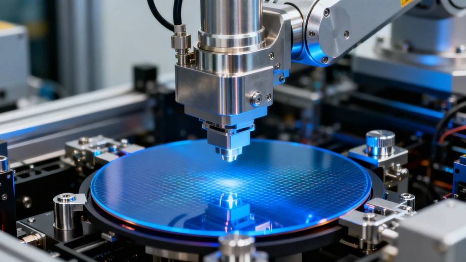
The relentless pursuit of miniaturization in electronics has reached a pivotal moment with the emergence of atomically thin materials, fundamentally altering semiconductor manufacturing possibilities. For decades, silicon-based transistors followed Moore's Law, but as features approach atomic scales, quantum effects and heat dissipation create insurmountable barriers. This technological impasse is driving manufacturers toward novel two-dimensional compounds that measure just one atom thick yet exhibit extraordinary electrical properties. Transition metal dichalcogenides like tungsten diselenide demonstrate ten times higher electron mobility than silicon, allowing electrons to traverse channels with minimal resistance and energy loss.
Remarkably, these materials enable radical simplification of fabrication processes while maintaining performance gains. Traditional chip manufacturing requires depositing and etching multiple material layers in vacuum chambers, an increasingly complex and expensive endeavor at nanometer scales. In contrast, two-dimensional semiconductors can be grown through chemical vapor deposition directly onto substrates, forming perfect crystalline structures with minimal defects. This breakthrough potentially reduces manufacturing steps by forty percent according to recent production trials, dramatically cutting costs and energy consumption per chip. While industrial-scale implementation remains challenging due to material uniformity requirements, pilot production lines have demonstrated viable yields for specialized applications.
A fascinating aspect of two-dimensional materials lies in their unique optical properties that could revolutionize photonic computing. Unlike opaque silicon wafers, atomically thin semiconductors are transparent yet capable of absorbing and emitting light with exceptional efficiency. Research teams recently demonstrated light-based transistors using molybdenum disulfide monolayers that switch states using photons instead of electrons. This convergence of electronics and photonics opens possibilities for optical interconnects that transfer data at light speed while eliminating copper wiring bottlenecks, potentially allowing future processors to exceed current speed limitations by orders of magnitude.
Manufacturers are strategically integrating these materials into existing infrastructure rather than pursuing complete overhaul. Hybrid architectures combining silicon backplanes with two-dimensional material components in critical circuit sections show particular promise. In recent prototypes, chip designers replaced conventional silicon transistors in memory modules with indium selenide components, achieving sixty percent faster data access while reducing leakage currents by ninety percent. This incremental approach provides performance gains without requiring entire fabrication plants to retool immediately, giving the industry crucial adaptation time.
Looking ahead, researchers focus on overcoming material manipulation challenges at industrial scales. Techniques like phase-change lithography show promise for precisely arranging these delicate monolayers into complex circuits without damaging their crystalline structures. As synthesis methods improve and manufacturing defects decrease, industry analysts predict two-dimensional semiconductors will capture twenty percent of specialty chip markets by 2028. Beyond computing, these materials hold transformative potential for sensors, flexible electronics, and quantum computing components, positioning them as foundational technologies for the next digital revolution.